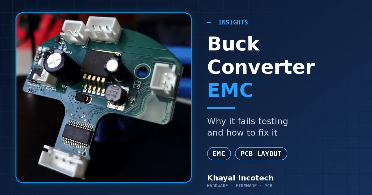
Buck converter EMC problems are one of the most common reasons a hardware product fails its first lab visit. The converter itself is usually fine. What fails is how it is placed, routed and connected to the rest of the board. Here is why it happens and what to check before you send a board for testing.
Switching converters are unintentional radiators, so in the US most products cover them through SDoC rather than an FCC ID. Our guide to FCC certification vs SDoC explains the difference, and our breakdown of what hardware certification actually costs shows what a failed visit does to a budget.
Why a buck converter radiates
A buck converter works by switching current on and off, usually somewhere between a hundred kilohertz and a few megahertz. Each switching edge is fast, and a fast edge carries energy at frequencies far above the switching frequency. Those harmonics are what show up on a spectrum analyzer.
The noise escapes in three ways. It radiates from the small loop of current that flows through the input capacitor and the two switches. It radiates from the switching node, the point where the switches meet the inductor. And it travels out along cables, which then behave like antennas.
The four mistakes we see most
The first is a large hot loop. The input capacitor and the two switches form a loop that carries sharp pulses of current, and the bigger that loop, the better it radiates. Place the input capacitor directly at the converter's input and ground pins, with the shortest path you can manage.
The second is too much copper on the switching node. That node swings between the input voltage and ground on every cycle, so a large pad or a long trace works like a small antenna. Give it only the copper the current needs, and keep sensitive traces away from it.
The third is a broken ground plane. Return current flows back underneath the signal it belongs to. If a slot or split sits under the converter, the current has to detour, and the detour becomes another loop. Keep the plane whole under the converter and its hot loop.
The fourth is an unfiltered cable. Noise on the supply or ground leaves the enclosure along the USB cable, battery leads or motor wires. Filter where the cable enters the board, using a ferrite bead, a common-mode choke or a small capacitor, depending on the product.
Cheap fixes at the design stage
Most of these fixes cost almost nothing before the board is fabricated, and a great deal afterwards.
Start from the manufacturer's reference layout. Converter vendors lay out their evaluation boards for low noise, so copy the loop geometry rather than inventing your own. Use a shielded inductor, since an unshielded one radiates a magnetic field into everything around it.
Choose the switching frequency on purpose. If your product has a radio, check that the converter's harmonics do not land in the band the radio listens to. Some converters also offer spread-spectrum modulation, which lowers the peak emission at any single frequency.
Finally, leave footprints for parts you might need later: an RC snubber across the switching node and an extra filter stage at the input. Leave them unpopulated. If the board needs them, you add them in minutes instead of respinning.
Test on your own bench first
A pre-compliance scan on the bench is not accredited and does not replace the lab. What it does is show which harmonics sit close to the limit while changes are still cheap. We run one before any board goes to a lab, because moving a capacitor on the bench costs nothing and a second chamber visit costs a lot.
If a harmonic sits near the limit line, change the layout or add filtering before you book the chamber.
Get the layout right the first time
Certification is designed in, not bolted on. If you are building a product with a switching converter, a motor or a charging port, talk to us about PCB design and layout before the board is fabricated.
Not sure whether your design will pass? Tell us what it does and we will tell you where the risks are.